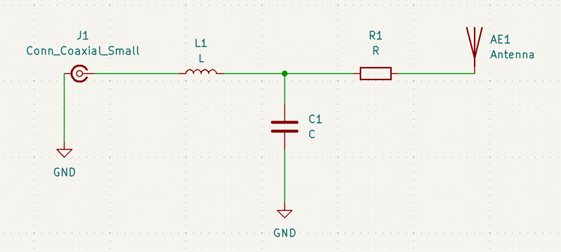
Our Expected Result in KiCad
If we pull this off with Zener, it should end up looking like the KiCad schematic below! You can follow along with the example GitHub directory.
 The first thing to do is import our dependencies. Diode kindly provides a few generics in the standard library that are very helpful for each of our physical components. Notably, our L Network uses an SMA connector, resistor, capacitor, inductor, ground, and antenna schematic symbol. We can easily import each of these schematics using the built-in
 Module() or load() function, coupled with the default package aliases, if the module is already available in the standard library.
However, for both our SMA connector and the antenna, the standard library does not provide a module, so we will need to create a module for each component ourselves.
Component or Module?
If you check the Zener module specification, you’ll see the following:
Each .zen file is a python module. It can be used in two ways:
-
Its exported symbols can be
load()ed into other modules. For example, load("./MyFile.zen", "MyFunction", "MyType") will load the MyFunction and MyType symbols from the MyFile.zen module.
-
It can be loaded as a schematic module using the
Module() helper. For example, MyFile = Module("./MyFile.zen") will import MyFile.zen as a schematic module, which you can instantiate like so:
MyFile = Module("./MyFile.zen")
MyFile(
    name = "MyFile",
    ...
)
.zen file that declares its inputs and creates components. So, with this knowledge, let’s define a component for our SMA connector and antenna.
The .zen file in which we write our component is technically a module. However, since a component must be defined within a .zen file, we will consider any file that specifies a component using the Component() syntax to be a component itself.
components directory in the root directory, where we can put both of our custom components.
It is convention to put the component’s .zen file inside of another directory with the same component’s name
Components
Now, if we think logically about a connector, we need one input and one output. What better construct than an io() declaration! Before we define our io()s, let’s first import a ground signal, which is require for the SMA connector to work. Then, let’s define our two ios for the connector, which by convention will be called In and Ext with a type of net:
load("@stdlib/interfaces.zen", "Ground")

# Declare io
In = io("In", Net) # Convention to name the variable and net the same
Ext = io("Ext", Net)
Library link: Connector:Conn_Coaxial_Small in the bottom left. Then, we can import the symbol with Zener (notice how we append .kicad_sym). We can do something very similarly for the footprint by looking around in ~/Library/Caches/pcb/gitlab/kicad/libraries/kicad-footprints/.... Last but not least, the standard library provides some layout functionality, so we can see a preview of the layout.
load("@stdlib/properties.zen", "Layout") # Import layout functions from the standard library
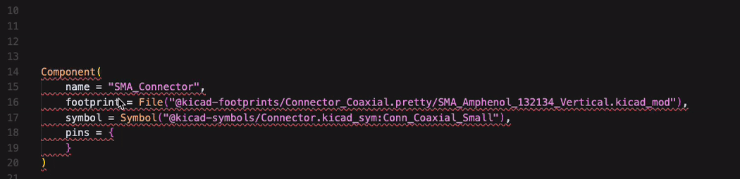
Component(
name = "SMA_Connector",
footprint = File("@kicad-footprints/Connector_Coaxial.pretty/SMA_Amphenol_132134_Vertical.kicad_mod"),
symbol = Symbol("@kicad-symbols/Connector.kicad_sym:Conn_Coaxial_Small"),
pins = {
"In": In,
"Ext": Ext
}
)
Layout(name = "SMA_Connector", path = "build/preview") # Don't use spaces in the name
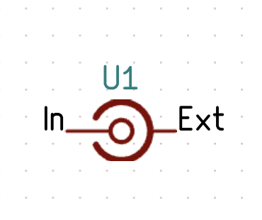
Hovering over the pins in a component definition will tell you all the pins Zener expects you to define.
load("@stdlib/interfaces.zen", "Ground")
load("@stdlib/properties.zen", "Layout")

In = io("In", Net)
Ext = io("Ext", Net)

Component(
    name = "SMA_Connector",
    footprint = File("@kicad-footprints/Connector_Coaxial.pretty/SMA_Amphenol_132134_Vertical.kicad_mod"),
    symbol = Symbol("@kicad-symbols/Connector.kicad_sym:Conn_Coaxial_Small"),
    pins = {
        "In": In,
        "Ext": Ext
    }
)

Layout(name = "SMA_Connector", path = "build/preview")
pcb: View Schematic button in VSCode:
 Pretty close! We might also want to change the prefix from U1 to J1 when we initialize the component. We can improve our
 SMAConnector.zen file by adding a prefix field to the Component() function and using a config.
load("@stdlib/interfaces.zen", "Ground")
load("@stdlib/properties.zen", "Layout")

In = io("In", Net)
Ext = io("Ext", Net)

prefix = config("prefix", str, default="J") # Add prefix from config

Component(
    name = "SMA_Connector",
    footprint = File("@kicad-footprints/Connector_Coaxial.pretty/SMA_Amphenol_132134_Vertical.kicad_mod"),
    symbol = Symbol("@kicad-symbols/Connector.kicad_sym:Conn_Coaxial_Small"),
    prefix = prefix, # Initialize component with prefix
    pins = {
        "In": In,
        "Ext": Ext
    }
)

Layout(name = "SMA_Connector", path = "build/preview")
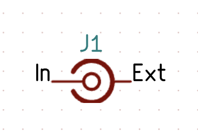 Even better!
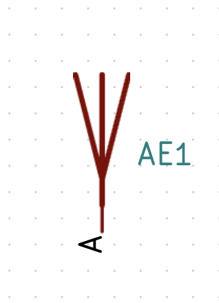
Similarly, for the antenna:
Even better!
Similarly, for the antenna:
load("@stdlib/properties.zen", "Layout")

A = io("A", Net)

prefix = config("prefix", str, default="AE")

Component(
    name = "Antenna",
    footprint = File("@kicad-footprints/RF_Antenna.pretty/Texas_SWRA416_868MHz_915MHz.kicad_mod"),
    prefix = prefix,
    symbol = Symbol("@kicad-symbols/Device.kicad_sym:Antenna"),
    pins = {
        "A": A,
    }
)

Layout(name = "Antenna", path = "build/preview")
Modules
While we could just instantiate a resistor, capacitor, inductor, and ground together on our PCB, it would make more sense for our matching network to be a module we can instantiate as a single unit. So, let’s make a seperate module for our matching network!
As per usual, let’s import the necessary modules we need from the standard library:
load("@stdlib/interfaces.zen", "Ground")
load("@stdlib/properties.zen", "Layout")
Capacitor = Module("@stdlib/generics/Capacitor.zen")
Inductor = Module("@stdlib/generics/Inductor.zen")
Resistor = Module("@stdlib/generics/Resistor.zen")
io()s:
io_IN = io("io_IN", Net) # Using "io_" is convention for io()s in modules
io_OUT = io("io_OUT", Net)
io_GND = io("io_GND", Ground)
Net()s for internal wires/signals:
L_IN = Net("L_IN")
T = Net("T")
io()s are for signals/wires that need to be accessed by other components or modules, while Net()s should be used for internal signals/wires that should not be exposed to external components or modules
io()s and Net()s we just defined:
Inductor(name = "L1", value = "10nH", package = "0603", P1 = io_IN, P2 = T) # Using placeholder values for value and package
Capacitor(name = "C1", value = "10pF", package = "0603", P1 = T, P2 = io_GND)
Resistor(name = "R1", value = "100ohm", package = "0603", P1 = T, P2 = io_OUT)
Layout() function, so the user can view the layout of the module in KiCad:
Layout(name = "MatchingNetwork", path = "layout/MatchingNetwork")
load("@stdlib/interfaces.zen", "Ground")
load("@stdlib/properties.zen", "Layout")

Capacitor = Module("@stdlib/generics/Capacitor.zen")
Inductor = Module("@stdlib/generics/Inductor.zen")
Resistor = Module("@stdlib/generics/Resistor.zen")

io_IN = io("io_IN", Net)
io_OUT = io("io_OUT", Net)
io_GND = io("io_GND", Ground)

L_IN = Net("L_IN")
T = Net("T")

Inductor(name = "L1", value = "10nH", package = "0603", P1 = io_IN, P2 = T)
Capacitor(name = "C1", value = "10pF", package = "0603", P1 = T, P2 = io_GND)
Resistor(name = "R1", value = "100ohm", package = "0603", P1 = T, P2 = io_OUT)

Layout(name = "MatchingNetwork", path = "layout/MatchingNetwork")
PCB
As we’ve done for both our custom components and modules, let’s import the necessary standard library functions into EX0001.zen:
load("@stdlib/interfaces.zen", "Ground")
load("@stdlib/properties.zen", "Layout")
MatchingNetwork = Module("//modules/MatchingNetwork.zen")
Antenna = Module("//components/Antenna/Antenna.zen")
SMA_Connector = Module("//components/SMAConnector/SMAConnector.zen")
Net()s:
IN = Net("IN")
OUT = Net("OUT")
GND = Ground("GND") # Ground is a special type of Net
Antenna(name = "Antenna", A = OUT)
MatchingNetwork(name = "MatchingNetwork", io_IN = IN, io_OUT = OUT, io_GND = GND)
SMA_Connector(name = "SMA_Connector", In = IN, Ext = GND)
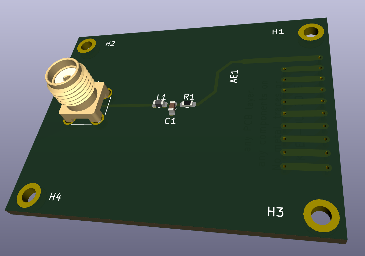
Layout(name = "Antenna_LRC_Matcher", path = "build/preview")
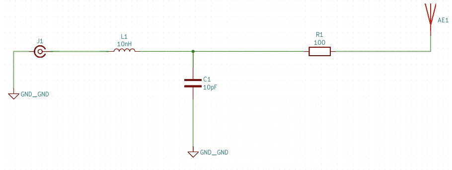 You’ve created a functional schematic with Zener!
Bonus
We can also programmatically add mounting holes with Zener:
load("@stdlib/interfaces.zen", "Ground")
load("@stdlib/properties.zen", "Layout")

MatchingNetwork = Module("//modules/MatchingNetwork.zen")
Antenna = Module("//components/Antenna/Antenna.zen")
SMA_Connector = Module("//components/SMAConnector/SMAConnector.zen")

IN = Net("IN")
OUT = Net("OUT")
GND = Ground("GND")

Antenna(name = "Antenna", A = OUT)
MatchingNetwork(name = "MatchingNetwork", io_IN = IN, io_OUT = OUT, io_GND = GND)
SMA_Connector(name = "SMA_Connector", In = IN, Ext = GND)

MountingHole = Module("@stdlib/generics/MountingHole.zen") # Import mounting holes from the standard library

for i in range(4): # Generate four mounting holes
    MountingHole(name = "H" + str(i), diameter = "M2")

Layout(name = "Antenna_LRC_Matcher", path = "build/preview")